Modules
IoT Device Development: Win in a Fast-Paced and Crowded Market
The global demand for connected devices is proliferating. Internet of Things (IoT) solution providers know that maintaining a status quo approach to IoT device design is less of an option as marketplace competition grows.
IoT companies are under constant pressure to create new products and enhance existing ones. These products must meet current needs while anticipating future use cases and requirements.
Enhance User Experience with Smart Modules
Being first to market with IoT products and services requires companies to monitor, explore and deploy emerging technologies to gain a competitive advantage. This constant innovation applies especially to IoT devices and services.
If you are not sprinting forward, you are moving backward. The latest and most discussed technologies are marketed heavily due to the urgency around IoT device development innovation. This urgency is also why companies move fast to invest in them, even if adopting innovative technology early comes with high risks.
Table of Contents
Approaches to IoT Device Development
In this crowded, competitive market with pressures inside and out, how can companies mitigate risks and save costs while maintaining an ambitious innovation pace?
Speed and quality are engineers’ number one trade-offs. Things like failures, delays and other unexpected events can go wrong. As a result, costs can soar, and the first-mover advantage can be lost.
There are three common approaches to IoT device development:
Chip Down
Build it piece by piece with various chips and components. This approach is the most time-consuming, complex and costly (see Figure 1).
IoT Module
An assembly of chips and circuits engineered to deliver a complete functional block operation (e.g., cellular communication). This approach is tested and certified as a fully integrated system. IoT modules enable a fast time to market. They simplify the development process and reduce costs (see Figure 2).
IoT Smart Module
A feature-rich module optimized for device development in which the solution supports elevated human interfacing with devices and data. Like IoT modules, smart modules are fully tested, certified and ready to use (see Figure 3).
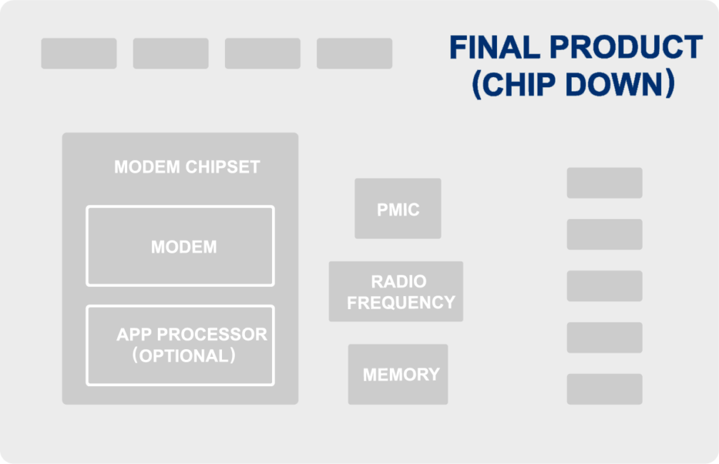
Figure 1: Chip down approach: Build the final product piece by piece.
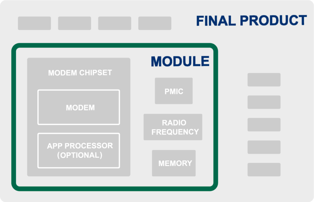
Figure 2: Module approach: Speed development with a prebuilt macro-component.
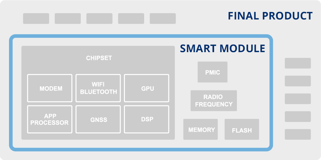
Figure 3: Smart module approach: Take advantage of additional development features.
A Closer Look: Chip Down vs. IoT Module Approaches
Chip down and IoT module approaches offer different benefits for IoT device development. Let’s take a closer look to gain a deeper understanding of significant differences, including:
- Time to market
- R&D knowledge base
- Resources required
- Risk profiles (e.g., delays, mistakes, issues and failures)
- Frequency and amount of human interfacing
Chip Down Approach
Embedding cellular connectivity with chip down is the lowest-level approach possible. It’s the lengthiest, costliest and most challenging. Every detail must be designed and tested, including all radio frequency (RF) engineering aspects. The chip down approach can take up to five years to complete.
In addition, your product must be certified. The cellular certification process comes with complexity and high costs. There are three layers of certification to plan for:
- Regulatory (e.g., FCC, CE, CCC, eMC, RED, Giteki and NAL)
- Industry (e.g., PTCRB and GCF)
- Network (e.g., Vodafone, Verizon, Telefonica, AT&T, T-Mobile)
Certification applications often fail in the first submission, meaning the product must be redesigned and go through the process again. The second submission may also fail. The process iterates until certification is complete or costs mount to the point that the product is no longer viable. It only takes two or three iterations to come to that.
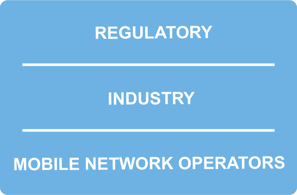
Figure 4: Three certification layers.
The bill of materials (BOM) of a product using the chip down approach may be slightly less expensive than one using the IoT module approach. However, there are fixed costs that must be amortized:
- R&D
- Certifications
- Delays
- Failures
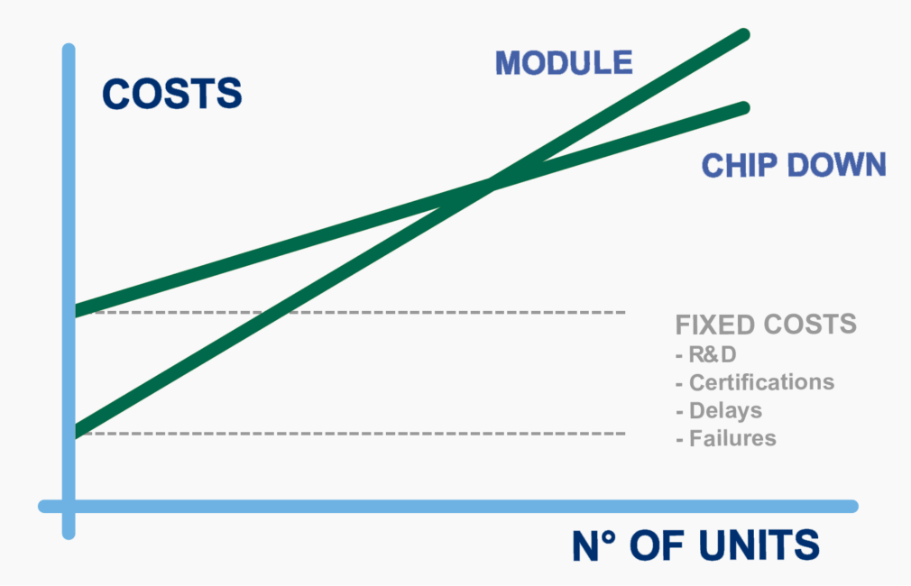
Figure 5: Chip down vs. module approach cost comparison.
If you expect to sell devices beyond the break-even volume calculation (see Figure 5), the chip down approach may be best from an investment perspective.
However, if the expected sales volume is not high enough, the fixed costs will not be amortized, and the project will not likely be approved. The time to market (which can be two to four times longer) may kill the project, even with high sales volume.
Module Approach
The module approach consists of designing a prebuilt system with components that include:
- Various chips
- The RF frontend
- Voltage regulator (PMIC)
RF is one of the most complex parts to manage and represents a critical advantage of using a module.
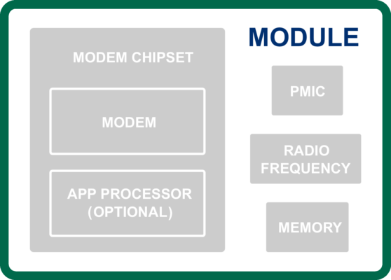
Figure 6: Example of module architecture.
Figure 6 shows cellular connectivity module architecture. An application processor may be available to run your apps, but not all modules will have this feature. When available, the application processor is fairly limited in capabilities, storage and memory.
The main advantage of the module approach over the chip down approach is clear: A module integrates your design as a regular component. It is fully tested, certified and ready to use.
Still, your product must be designed and tested. It may require some final certifications. However, many individual tasks of the chip down approach will already be completed.
The Smart Module Approach and the Human Factor
Some IoT device projects must include an external host central processing unit (CPU) and some memory in the product along with the module (see Figure 7).
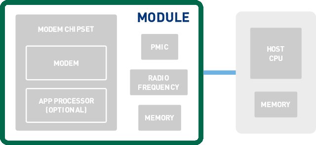
Figure 7: Module with a host CPU.
There are several use cases in which this added processing power may be required. One of the most frequent uses cases is when your device must support a complex human interface array, including:
- Touch screens
- Multiple cameras
- Video encoding and decoding
These IoT applications are prime targets for the smart module design approach. They include all devices that incorporate advanced human-machine interfaces (HMIs).
Smart Module Use Cases
- Point of sale (POS)
- Vending machines
- Smart thermostats
- Home panels
- Smart doorbells
- Electric vehicle (EV) charging stations
- Dashcams
- Smart mirrors
- Cameras with image recognition
- PDAs
- Tablets
- Drones
- Robotics
- Augmented and virtual reality
- Gaming
A consumer-class operating system (OS) is at the core of high-performance HMI device development. Android™ is the most open of the top two in the market and runs on top of most IoT smart modules.
This OS hastens development times and allows engineers to focus on the app software instead of the hardware.
Why and When to Choose a Smart Module
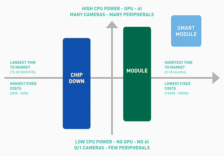
Figure 8: Smart module positioning.
Smart modules are ideal for your IoT deployment if:
- You are building a multimedia-rich device with many peripherals.
- You are not going to sell millions of items, at least initially.
- You must complete the product and app software quickly (i.e., you do not have years to design, test and certify in the chip down or IoT module approaches).
IoT smart modules are tested in the production line. Test results are recorded and tracked. Any problems arising after manufacturing the end device can be identified and resolved easily.
Smart modules reduce all core electronics to one stock-keeping unit (SKU) and one vendor. This reduction simplifies development and maintenance and reduces the total cost of ownership (TCO).
Smart modules empower you to focus on software development instead of hardware. They enable developers to design hardware and software at a pace that is unattainable with other approaches.
Estimating Time to Market and Savings
Chip down, IoT module and smart module approaches offer advantages and disadvantages. Selecting the best approach for your IoT project will depend on:
- The type of device
- Knowledgebase
- Budget
- Expected sales volume
- Sensitivity to delays and cost overruns
Consider all layers of variable and risk costs, including:
- Certifications: Telcos, industry, regulatory
- Errors: They happen quite often in R&D, especially with recent technologies
- Supply chain issues: The more suppliers there are, the greater the risks
- Entering (too) late in the market: You lose the revenue peak of being the first to market and the opportunity to become the market leader
Table 1 summarizes the differences between the three approaches in terms of time to market and costs. Our R&D, product management and technical support leveraged experience with our customers and market to create these estimates.
| Approach | Chip Down | Module | Smart Module |
| Estimated Total Development Cost | $5,000,000+ | $200,000-$500,000 | $50,000-$100,000 |
| Time to Market (Years) | Up to 3 | 1-2 | 0.5-1 |
Conclusion
Long development cycles are no longer sustainable with the accelerated emergence of new use cases and IoT technologies. The good news for IoT device developers is that IoT module and smart module options are available to shorten the path to market.
Companies must understand the costs and benefits of the chip down, module and smart module approaches to make the best possible use of them. Businesses that assess needs before building an IoT device will see reduced risk and faster returns on investment.
Appendix
Build a Prototype with Our Smart Module Evaluation Board
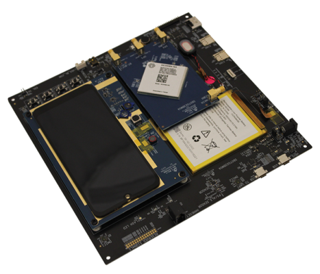
Our IoT smart module evaluation board (see Figure 9) is designed for engineers, programmers and developers to:
- Quickly develop and test applications based on current and future smart module families leveraging Android
- Debug and improve Android applications based on our smart modules
This evaluation board is a complete peripheral-rich system to develop and test new products.
- Two cellular antennas
- Four RF cable adapters (female SMA connector to U-FL)
- One GPS passive antenna with a cable and male SMA connector
- One Wi-Fi dual-band antenna with a male SMA connector
The evaluation board peripherals include:
- Touch screen (LCM)
- Proximity sensor and ambient light sensor
- Accelerometer (G-Sensor)
- Three cameras (front and rear)
- Analog and digital audio
- Two SIM card holders
- One USB interface
- Two UART ports available on a USB hub adapter (for debugging)
- Four buttons (Power Key, Reset, VOL+ and VOL-)
- TransFlash (TF) card interface
- Battery charger
A demo app for controlling the light, proximity and accelerometer sensors is provided to assist development. It is available as source code, so developers can easily study the code and focus on building apps.